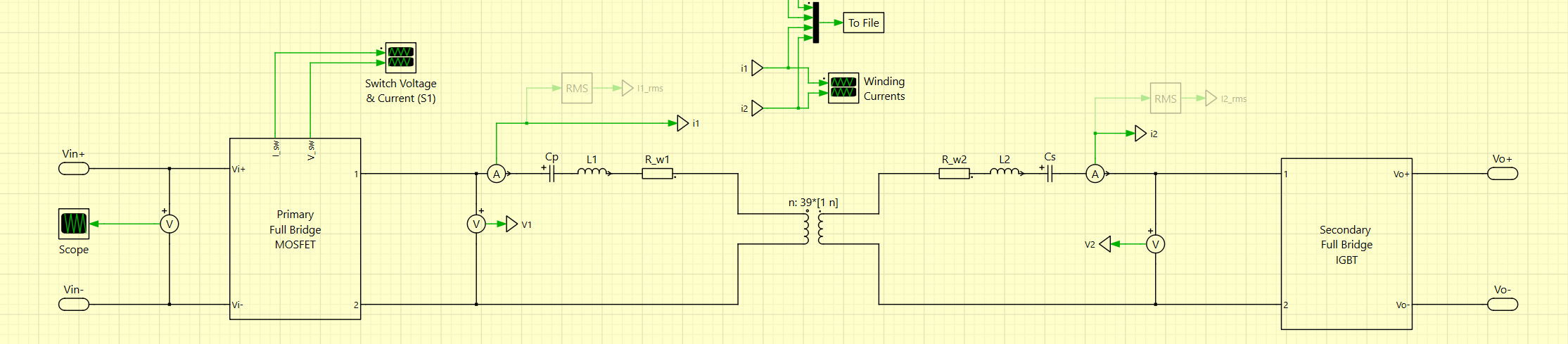
I am simulating a circuit with two full bridges (primary with MOSFETs and secondary with IGBTs) shown in the image.
I use ‘MOSFET with diode‘ and ‘IGBT with diode‘ for the parts. In the thermal models I use, body diode conduction is included by entering negative values for conduction that correspond to body diode conduction parameters in the datasheet.
In the circuit, I am trying to only have the antiparallel diodes conduct on the secondary full bridge by having the duty cycles of the switches set to zero. When I do that, the results do not correspond to when I have a diode full bridge or an active switch full bridge with gate control signals.
I know that with MOSFETS, I can enable “use gate dependent conduction losses” in the conduction losses portion of the thermal model, but I do not seem to have that option for IGBTs. I think this is why the results do not agree. I may be wrong on this.
I am wondering if there might be a thermal model implementation caveat with the “IGBT with diode” that I am not adhering to, and would be grateful for troubleshooting insights.
An IGBT can only conduct in the first quadrant and its antiparallel diode only in the third. They cannot conduct at the same time, which is why the option “Use gate dependent conduction losses” is not available. For a MOSFET, reverse current can also flow through the channel, so simultaneous conduction of the body diode and MOSFET channel is possible. That is why this option exists there.
From your description it is not fully clear whether “the results do not correspond” refers to the electrical behavior or the thermal loss calculation. To understand what is happening in your case, it would be helpful if you could share your model.
Thank you for your response. By saying that “the results do not correspond”, I was referring to the system’s electrical behavior.
I have attached the file and thermal models of the devices I am using. In the PLECS file, I have a “Secondary full bridge - zero duty cycle” block and a “Secondary full bridge non-zero duty cycle block” inside the “Converter” subsystem. It currently has the zero duty cycle block connected, and the other commented out.
I initially had the non-zero duty cycle connected, and that gives me the behavior I am looking for, but when I changed it to its current version to compare performance when conduction is through IGBT antiparallel diodes, the electrical results are very different. The non-zero duty cycle block can be connected and the other commented out so that expected behavior can be viewed.
This issue appears to be related to the currently selected configuration (IGBTs with zero-duty cycle), which seems to be incorrectly implemented. The signals do not exhibit a PWM pattern, however, the low-side signals remain constantly on rather than turning off. When I disconnect all the Signal From blocks, I obtain the same waveforms as if only diodes were used.
As a suggestion, I recommend using Configurable Subsystems for this type of analysis. Since you can directly select the configuration, there’s no need to comment or uncomment subsystems, making the process much faster and more efficient.