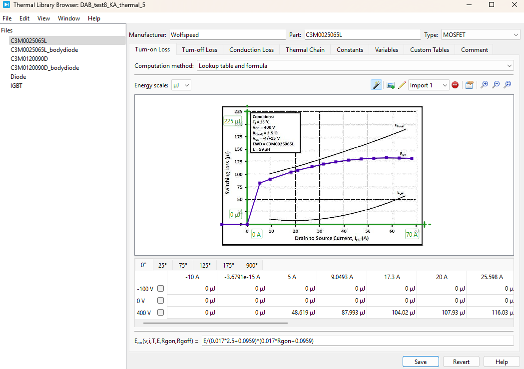
I am looking at the conduction and switching losses of the wolf speed C3M0025065L FETs. I used the thermal curve fitting to import the the turn-on and turn-off characteristics of the FETs
When I calculated the switching loss per FET using the data sheet (given below) I get Psw = Etol*f = 15W per fet. But in my simulation I get a much lower number I get about 4W.
Can someone please explain if this is a glitch in the thermal data provided by the manufacturer ? Or simulation is not reading the correct values from the graphs ?
I’m curious why you are not using the thermal description XML files that Wolfspeed already provides for PLECS for its devices, and instead importing the datasheet curves yourself?
Further, can you post your PLECS circuit model? If not, can you show probed voltage current and temperature waveforms for one of the devices so we understand where you are operating within the curves? Have you checked to be sure that the body diodes are actually conducting in your model?
Hi Kris,
I used the XML files that wolf speed has already given to do a sanity check but still the numbers look the same. So I guess importing the curves did not change anything.
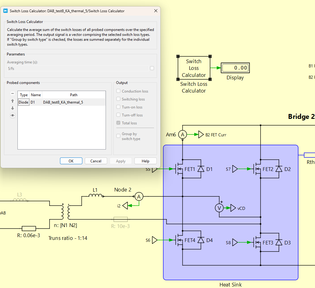
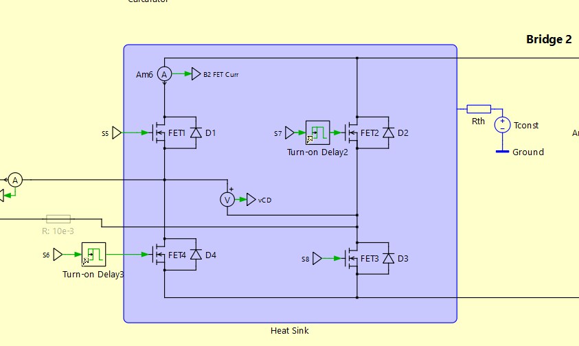
I looked at the current waveforms through the diode, seems like its not conducting during the turn off of FETs.
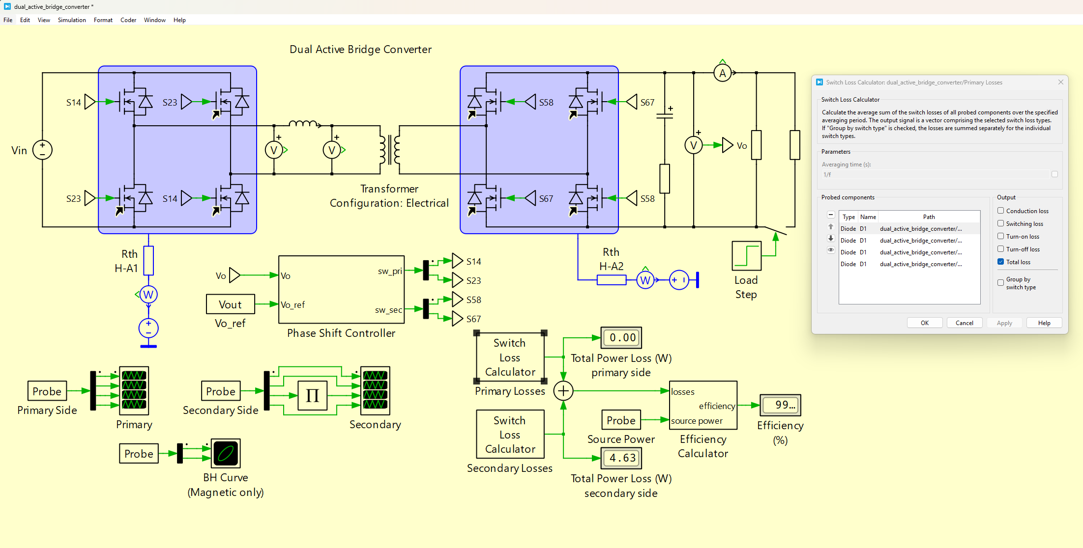
I see the same issue with the PLECS DAB demo model, in that also current through diode is zero.
In the DAB demo model, the forward voltage of the body diode leads to the third-quadrant current entirely going through the MOSFET channel. You can remove or adjust the forward voltage to allow the diodes to conduct, but then you also have current sharing between the MOSFET channel and body diode as defined by the resistor divider of the two on-resistance values.
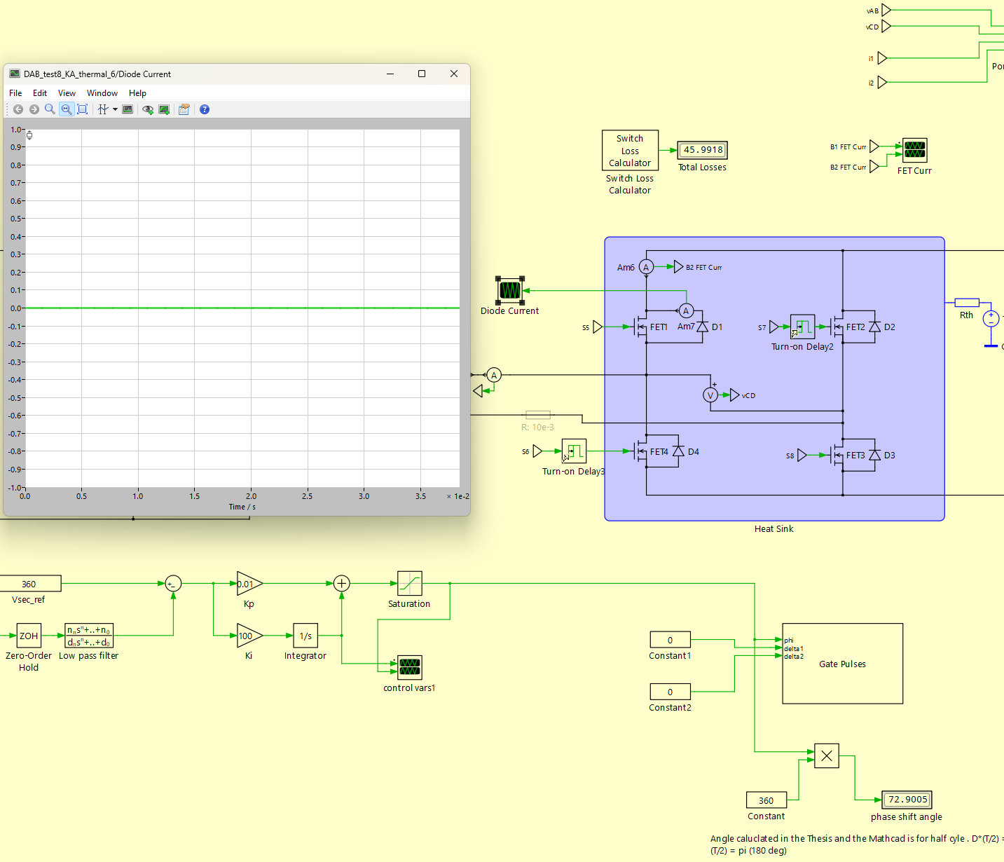
I see, because the currents are going through MOSFET channel the diode is not conducting. Is that right ? So if we change the Vf it will be a different value from the value given in the datasheet. So I am using Vf as 0.5V and the diode starts conducting. But this Vf is 10x smaller than datasheet specified Vf value…
Simulation:
In my DAB design that I shared earlier; the wolfspeed data sheet the Vf is 5V. When I change the Vf to 0.5V the diode starts conducting and shows conduction losses, when the FET is in its dead time. But now the FET does not conduct at all. And this is same in the DAB Plecs Demo Model as well.
I think what’s most appropriate to be concerned with here is what is typical in the real application and then to get your model to replicate that as closely as possible. And that might deviate from what you see in our demo model, admittedly, as tuning on-resistances and forward voltages for your actual steady-state condition, operating temperature, etc. will likely lead to unique values.
My understanding is that in the real application in a general sense, when the gate is on during third quadrant conduction the majority of the current should go through the channel, and Wolfspeed has characterized the MOSFET third-quadrant conduction losses to be the parallel sum of losses from channel and body diode (so you should want the current to entirely go through the channel in this condition). Of course, during dead time when the gate is off, the current should entirely go through the body diode. So I expect that if you were to add a dead time/turn-on delay to your switching signals that you would also see this behavior.
I changed the Vf to 0.35V (5V is the datasheet given Vf) to get the power loss from simulation to be equal to what I see from my calculations (calculated from the data sheet graphs). However this manually entered Vf is x14 smaller than the data sheet.
I wonder if this is a issue with plecs MOSFET or if its a wolfspeed part thermal library issue. Please advice for future simulations. And Thank you so much for your help Kris
I would say this is not an issue with PLECS nor a Wolfspeed issue per se, but more a modeling challenge in general. Specifically because Wolfspeed’s third quadrant conduction data includes the influence of the parallel body diode losses when the gate is on and the channel is conducting, it actually doesn’t make sense to allow current to flow through both paths at the same time (and reduce the current in the channel, thus giving an inaccurate loss calculation). So the body diode forward voltage allows you to manipulate what happens in that case. Other vendors may only provide third quadrant MOSFET conduction loss data that is inclusive of the contribution from the channel, however, for example.
Eventually Wolfspeed will release an updated PLECS library that uses a single, combined MOSFET with Diode component where the forward voltage is still included, but the two separate paths for channel and body diode, each with their with on-resistance, will be reduced to one. And hopefully that both reduces confusion and makes everything more efficient for the user.
One last thing, I understand the 14x discrepancy might seem concerning, but there are other ways in theory to get around this. For example, you could add a controlled voltage source in series with the diode that is either 0V if the gate is on or the full 5V if the gate is off. See below for a diagram of how that could be done:
Of course, if the Vf = 0 and you have Ron defined for the MOSFET and diode you would still get current sharing, so you then might consider Ron_MOSFET = 0 and Ron_diode > 0, or try other ideas. You could also decide how important these parameters are to your system-level simulation results (e.g., the influence of the on-resistances may be negligible).
Thanks Kris! I will give it a try with the controlled voltage source.
It is quite important in my DAB design because I am looking at about 300A going through the FET when its on.
I tried the voltage source approach it does not work. It gives the same results as if I had the Vf=5V and all the conduction happen through the MOSFET even during dead time. And zero conduction loss in the diode.
Anyway thanks for the help Kris!!
Then you might need to also have the “NOT” of the gate signal feed an on/off switch in series with the MOSFET to open circuit that path when the diode is conducting. These suggestions are definitely more in the realm of “hacks” so you will need to experiment to figure out what is the desired behavior you need, or you can manipulate the forward voltage as you mentioned originally.