Hi Nishan, maybe a workflow like the following might be an option for you:
- using a configurable subsystem, setup a configuration where you use parasitic capacitances and no thermal losses to capture if your system achieves ZVS or not across a few operating conditions. you could use this model to validate if your analytical model matches simulation results.
- if you also want thermal simulation then you could have a configuration that uses ideal switches + thermal loss data with a scaling factor (based on your previous test) to capture the thermal impacts of ZVS.
Something to consider to make your life easier:
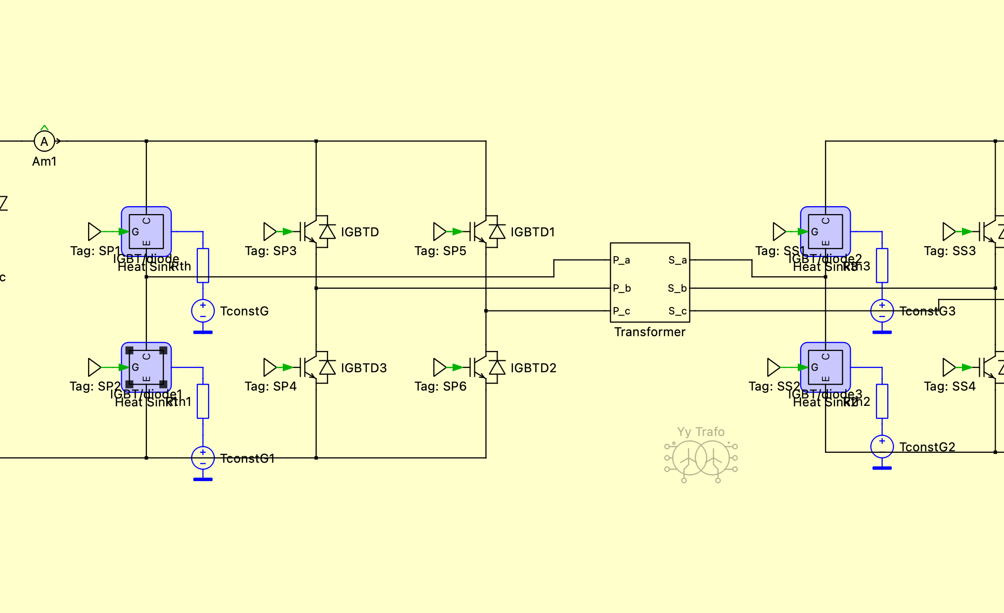
If you decided to start experimenting with configurable subsystems you might benefit from the usage of model reference. See section 7 of this document. This way you don’t have to maintain 4 separate modules here but only have to make changes to 1 module as you start tinkering. E.g. IGBT/diode subsystem being driven by SP1 could be the reference module and all other submodules could use model references.
Finally, I don’t have a lot of experience with DAB converters but having worked extensively with flyback converters I have found that the Coss is not the only contributor to the parasitic capacitance that needs to be discharged for ZVS. It is a good starting point but just wanted to make you aware as you might see a different result in the lab. For the flyback, the approach I took was:
- measure the magnetizing inductance of the flyback converter with an LCR meter
- operate the HW flyback converter deep in DCM and measure the primary switch drain to source voltage ringing frequency in DCM
- back calculate the node capacitance based on the above measurements → effectively I lumped all the parasitics capacitances like your Coss, transformer winding capacitances, etc
I then utilized PLECS to determine what the system would need to achieve ZVS operation for an active clamp flyback (e.g. what drive duration for the clamp switch, dead-time between clamp switch and main switch, etc).
Hope this helps!