Hello,
I am trying to implement the operation of ZVS turn on in the switches of a single phase DAB converter. Under single phase shift control and matched voltage ratios (transformer turns ratio matches with the DC terminal voltage ratio), the converter should inherently facilitate ZVS turn on for all the switches.
However, there are some conditions that need to be satisfied for this to happen.
-
At the moment of turn on, the anti-parallel or the body diodes of those switches need to be conducting.
-
For this to happen, the C_oss capacitances in each switch pair (which is abuout to turn on) needs to be discharged by the leakage inductance of the transformer during the deadtime. This is because, during the previous switching instance (where the opposite two switches are conducting), the nodes are clamped with DC link voltage allowing the C_oss to charge and have a voltage across them.
So I want to show this on PLECS. Which means, I want to show that ZVS turn on may happen when these conditions are met, and show that hard switching happens when these are not met. Unfortunately, I do not have an idea to implement this.
The reason lies mainly with not knowing how to integrate the effect of C_oss to the switching operation. I do not want to add capacitances parallely as well since it would slow down the simulation (this is the main reason I switched to PLECS from Simulink. The simulation becomes really slow). I need to know there is a way to do this through look-up tables or some faster way.
I modeled the thermal system of the switches with look-up tables as PLECS supports, with a clear operating point of 0 losses when the voltage or the current at 0. But, the system does not work as expected. It always gives me ZVS turn on whenever I use some deadtime between the switching which is quite inaccurate. And whenever I do not provide any deadtime, it shows me that a turn on switching loss is happening according to the look-up tables.
How can I model the system while accounting for those conditions as well? Any sort of suggestion will be appreciated.
Thanks,
Nishan
Hi Nishan,
Could you share your model with the community? That would make it easier to follow exactly what you’re referring to in your question. Right now, I’m having a bit of trouble visualizing the challenge you’re describing, especially your last comment:
“I modeled the thermal system of the switches … according to the look-up tables.“
Hello,
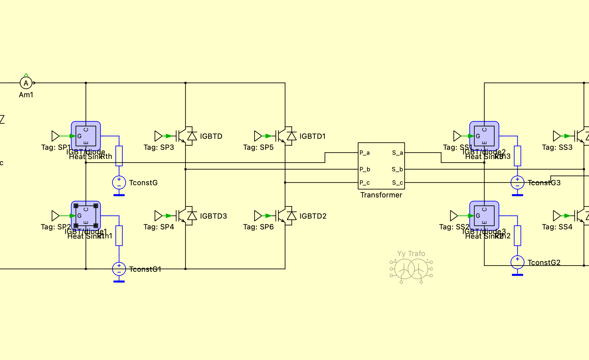
Thanks for the response. Herewith I have attached the model which I am working on. Please let me know if you need further information.
Thanks
DAB_plecsupport.plecs (265.8 KB)
Also, here are the corresponding thermal files of the semiconductors I have been using
FF150R17KE4_diode.xml (9.3 KB)
FF150R17KE4_igbt.xml (12.9 KB)
Hi Nishan, thanks for the info - really helps visualize the issue you are describing.
Here are some questions:
- [So I want to show this on PLECS. … idea to implement this.] - in your application are conditions known for when ZVS is achieved in your converter or is this something that needs to be determined via simulation? If you know the conditions for ZVS operation then potentially you could use a variable that indicates whether ZVS is achieved or not based on the operating condition and utilize this with your switching loss lookup take (see Switching losses in partially soft-switching inverter - #2 by Oliver_Schwartz)
- If however, you don’t know prior to running your simulation which operating conditions will achieve ZVS, then I can’t think of a way how PLECS would be able to predict this for you without including the node capacitor of the switches.
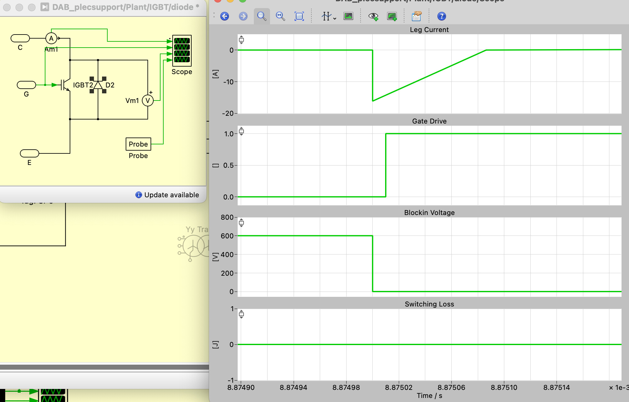
- [I modeled the thermal … according to the look-up tables.] - this is because the PLECS thermal domain will use the blocking voltage right before turn on, the conducting current right after turn on and then use the lookup table to determine the losses.
When I probe some waveforms in your topology I see that when the gate turns on the block voltage is already zero (likely because the body diode is conducting prior to turn on). Thus the lookup table at the turn-on will always show 0J of switching energy at turn on as the blocking voltage is 0V as the gate turns on (see below).
Hi Munadir,
Thank you for the response. I also went through the thread you mentioned.
My objective is this, I am studying an analytical method to determine whether a certain semiconductor device alongside a defined DAB operating condition would be able to facilitate ZVS turn on. So, I am using PLECS as a method of validation for that process.
Theoretically, during the deadtime, the C_oss or the output capacitance of the switch (which is about to be turned on) needs to be fully discharged by the current which was flowing across the leakage inductance due to the previous switching state.
What I did was, I modeled the thermal network of the switches using the .xml file provided by the manufacturer and added some extra 0 points to avoid the negative energy error. However, I did not model any parasitic effects of the semiconductor. Just modeled the losses using look-up tables (as per the xml file)and added a heatsink to determine the rise in the junction temperature.
The issue comes after this. I was wondering how to simulate the operation of C_oss discharge during the switching. As you mentioned in the “blocking voltage“ plot, it suddenly goes to zero during the deadtime, rather than showing it as a capacitive discharge. This affects the accuracy of what I want to see. I want to see how the ZVS turn on depend on
- The current which was flowing through the inductor
- The amount of deadtime
- The size of the inductance
So, if the blocking voltage goes instantly to zero, then there is no effect from either of these parameters which I am trying to observe. ZVS turn on happens either way when we provide a small bit of deadtime.
I can also think of adding a capacitor across the switch to represent the C_oss, but I sort of refrained from doing it as it would slow down the simulation. Just wanted to see whether there is any other effective trick which can be used to make this work while maintaining the switching speed.
As per your instruction, seems like there isn’t any. However, appreciate your feedback and time over this matter.
Nishan
Hi Nishan, maybe a workflow like the following might be an option for you:
- using a configurable subsystem, setup a configuration where you use parasitic capacitances and no thermal losses to capture if your system achieves ZVS or not across a few operating conditions. you could use this model to validate if your analytical model matches simulation results.
- if you also want thermal simulation then you could have a configuration that uses ideal switches + thermal loss data with a scaling factor (based on your previous test) to capture the thermal impacts of ZVS.
Something to consider to make your life easier:
If you decided to start experimenting with configurable subsystems you might benefit from the usage of model reference. See section 7 of this document. This way you don’t have to maintain 4 separate modules here but only have to make changes to 1 module as you start tinkering. E.g. IGBT/diode subsystem being driven by SP1 could be the reference module and all other submodules could use model references.
Finally, I don’t have a lot of experience with DAB converters but having worked extensively with flyback converters I have found that the Coss is not the only contributor to the parasitic capacitance that needs to be discharged for ZVS. It is a good starting point but just wanted to make you aware as you might see a different result in the lab. For the flyback, the approach I took was:
- measure the magnetizing inductance of the flyback converter with an LCR meter
- operate the HW flyback converter deep in DCM and measure the primary switch drain to source voltage ringing frequency in DCM
- back calculate the node capacitance based on the above measurements → effectively I lumped all the parasitics capacitances like your Coss, transformer winding capacitances, etc
I then utilized PLECS to determine what the system would need to achieve ZVS operation for an active clamp flyback (e.g. what drive duration for the clamp switch, dead-time between clamp switch and main switch, etc).
Hope this helps!
Hi Munadir,
Thank you for the response and the guidance. I will look into that.
Also, thanks for your insights on the parasitic estimation as well. Appreciate that.
BR, Nishan