Good day! I am currently working on an LLC resonant converter to be implemented using PLECS. In the lab, we currently have an RT Box, a TI F28069 LaunchPad, and a LaunchPad-Nucleo Interface board.
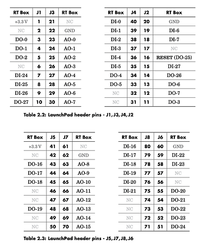
I would like to utilize the analog outputs (AO) to plot the waveforms (e.g. resonant current, square wave voltage, etc.) with an oscilloscope. While there are BNC ports for the AO ports for channels 0-7, we do not have any male BNC-BNC cables. Then, I came across the RT Box LaunchPad-Nucleo Interface manual which shows the pinout of the LaunchPad which contains the AO ports for channels 8-15 as seen here.
With these concerns in mind, my questions are the following:
-
Can the pins from the jumpers of the TI LaunchPad be used as AO and plot the signals with an oscilloscope? Thereby not using the BNC ports of the interface board.
-
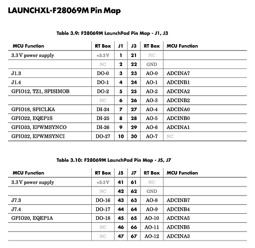
If so, how can I set the LaunchPad to use the RT Box pinout instead of its MCU function as shown here.
Your responses will be greatly appreciated. Thank you very much!
Edit: Here is the PLECS file that I made so far.
LLC + PWM.plecs (48.8 KB)
Firstly I want to point out your RT Box model is not configured correctly, indicating a refresh on some key real-time modeling concepts is required:
- Please review the “From Offline to Real-Time” and “Solver Engines” RT Box Tutorials.
- There also is a TI C2000 Demo Model Titled “LLC Resonant Converter” - please review how the RT Box model is constructed.
- Most importantly, you should be using the Full-Bridge LLC Converter from the Electrical + Nanostep section of the PLECS Library. The LLC will then be modeled with a 7.5 nanosecond step size on the RT Box CE you are using, significantly improving the model fidelity.
- Eliminate the boolean data conversion, which will significantly compromise the accuracy of your real-time model.
- Your RT Box Step size set in the Coder Options + Scheduling tap is 2 msec, which is not appropriate for a converter operating at a 100 kHz switching frequency (2-3 usec is more appropriate for an RT Box CE).
(e.g. resonant current, square wave voltage, etc.) with an oscilloscope
The analog outputs of the RT Box CE (which is what your model is configured for) will update at the CPU step size (suggested at 2-3 usec above). The resonant current and output voltages will be shown with this level of resolution and so the waveforms will be significantly downsampled compared to the Nanostep solver’s step size of 7.5 nsec.
The next major PLECS 5 release will include a Nanostep Scope functionality, which will allow users to have a real-time software-based scope in your PLECS model with the Nanostep solver’s resolution. This will run on your existing hardware with a firmware upgrade. Until then you will not get the quality of output signals you are expecting. There also is the RT Box 4 which as has dedicated Analog Outputs for Ultra-Low Latency Performance specifically targeting Nanostep topologies.
Can the pins from the jumpers of the TI LaunchPad be used as AO and plot the signals with an oscilloscope? Thereby not using the BNC ports of the interface board.
Yes, you can connect your oscilloscope directly to the C2000 header pins with a probe.
If so, how can I set the LaunchPad to use the RT Box pinout instead of its MCU function as shown here.
The tables show what C2000 Pin connects to which RT Box pin. Your model shows you are using the 28069. See the appendix of the interface manual which shows the pin-mapping for that specific MCU. For example you can see that the MCU EPWM1A uses GPIO0 by default. The interface board maps the C2000 GPIO to the RT Box Digital Input channel 0.
Thank you very much for the reply! Sorry for the delay on my end but I have a few clarifications on your response.
Most importantly, you should be using the Full-Bridge LLC Converter from the Electrical + Nanostep section of the PLECS Library. The LLC will then be modeled with a 7.5 nanosecond step size on the RT Box CE you are using, significantly improving the model fidelity.
My only concern is that I need to plot the full bridge inverter output voltage and unfortunately the signals from the Full-Bridge LLC Converter component does not include it and I require the said signal. Is there a way to plot the inverter voltage using the said module?
The tables show what C2000 Pin connects to which RT Box pin. Your model shows you are using the 28069. See the appendix of the interface manual which shows the pin-mapping for that specific MCU. For example you can see that the MCU EPWM1A uses GPIO0 by default. The interface board maps the C2000 GPIO to the RT Box Digital Input channel 0.
How about for analog outputs say for AO-8 where I want to plot the capacitor voltage or any waveform of the LLC to the oscilloscope. Once the C2000 is connected to the interface board, is the pin 63 in J7 set to AO-8 instead of ADCINB7?
Attached here is the picture of the setup in the lab for your reference. Thank you again!
Is there a way to plot the inverter voltage using the said module?
With the RT Box 4 hardware and forthcoming Nanostep Scopes, users will be able to measure certain internal Nanostep signals. In the current releases of PLECS, you do not have this level of fidelity, but you can determine the inverter output voltage of the Nanostep component from the input voltage and applied gate signals.
If you do not use the Nanostep component you can plot “a voltage” but your results will be have such a high level of error that they will not be meaningful for your investigations.
Once the C2000 is connected to the interface board, is the pin 63 in J7 set to AO-8 instead of ADCINB7?
When the interface board is connected, an RT Box Analog output is wired to the C2000’s ADC input. The pin serves both purposes - the RT Box drives the analog output which is then sensed by the C2000.
Good day, Bryan!
Thank you very much for your support! I was able to plot the signals such as the resonant current and magnetizing current of the LLC resonant converter thanks to your suggestions and modifications. Attached here is the PLECS scope of the signals and their corresponding output in the oscilloscope.
Though not fully replicated, I suspect it is because of the limitation imposed by the RT Box CE here in the lab which is only limited to the micro-scale in terms of its resolution.
As for the square wave voltage I mentioned previously, I tried to derive it using circuit analysis via applying derivatives to current waveforms and was not able to obtain the desired signal. I do hope PLECS 5 will release very soon though.
Attached here is the modified PLECS file as well. Thank you so much!
LLC + PWM.plecs (72.3 KB)
Great, thanks for the update! It looks like you were able to achieve a 1 usec step size with the RT Box CE, and with a 100 kHz PWM there’s 10 samples per switching period, giving quite reasonable looking (but obviously discretized) waveforms.
I’ll note with the RT Box 1 and CE you could also approximate the mid-point voltage with something like the circuit below - noting that the calculation updates at the CPU step.


