Introduction
Advanced control strategies for LLC resonant converters promise improved dynamic performance and robustness, but their practical realization often requires significant effort to transition from offline simulation to embedded hardware. PLECS addresses this challenge by providing a unified workflow spanning system-level modeling, code generation, and Hardware-in-the-Loop (HIL) validation, allowing engineers to move efficiently from concept to real-time implementation.
A previous article, Small-Signal Modeling and Control of LLC Resonant Converters in PLECS , introduced multiple charge control strategies for LLC converters, including both single-ended and dual-ended implementations. These approaches enable the use of a simple PI controller in the outer voltage loop while producing plant dynamics that remain largely invariant across input voltage, output voltage, and load conditions. That article focused on system-level modulator definitions and serves as the foundation for the work presented here.
In this article, we extend that work by demonstrating a complete real-time realization of dual-ended charge control on a TI C2000 microcontroller using the PLECS Target Support Package (TSP), followed by closed-loop validation using a PLECS RT Box 4. This enables rapid verification of the full control stack, from modulation to supervisory logic, without requiring physical power hardware.

Real-Time LLC Plant Modeling with RT Box and Nanostep
PLECS RT Box enables HIL validation of power electronic controllers operating at high switching frequencies. In this example, the power stage is modeled using the PLECS Half-Bridge LLC Converter Nanostep library module. The converter is connected to an ideal DC voltage source at the input, while the output is modeled as a resistive load with a filter capacitor.
For HIL testing of the MCU implementing dual-ended charge control, measurements of the DC input voltage, DC output voltage, and resonant capacitor voltage are required. The input and output voltages are sampled by the MCU ADC and exhibit relatively slow dynamics due to the bus capacitors, so they are provided through standard analog outputs. In contrast, the charge control algorithm relies on the resonant capacitor voltage on a cycle-by-cycle basis. This signal must therefore be reproduced by the HIL system with very high bandwidth, timing accuracy, and resolution, which is achieved using the RT Box 4 Nanostep DAC outputs with 8 ns update capability.

The resonant capacitor voltage is an internal state of the PLECS Half-Bridge LLC Converter Nanostep library module and is accessed using the Nanostep Probe block. This signal is routed directly to a Nanostep DAC output on the RT Box 4, allowing the MCU hardware comparators to operate on a high-fidelity, real-time representation of the resonant waveform. This enables true cycle-by-cycle validation of dual-ended charge control, where each switching transition is determined directly by the comparator detecting a resonant capacitor voltage crossing its reference, rather than being dictated by a PWM compare event as in traditional direct-frequency control strategies.
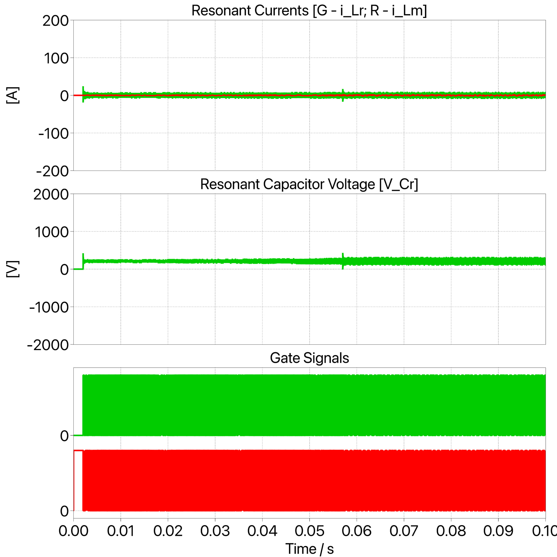
Output voltage and current are monitored using standard PLECS Scope blocks, while resonant tank currents (leakage and magnetizing), resonant capacitor voltage, and gate signals are visualized using the Nanostep Scope. During HIL operation, PLECS can capture signals on the target device and display them using standard Scope blocks, effectively functioning as a soft scope. The Nanostep Scope also allows internal Nanostep variables to be observed via External Mode.
This setup enables direct observation of the controller’s performance in HIL mode, as described in the following sections.
Dual-Ended Charge Control Implementation on TI C2000
Modulator Operation
At its core, the dual-ended charge control modulator operates as a two-state machine:
-
High-Side On: The high-side switch is turned on and the reference ramp for the high-side comparator (CMPH) is reset. The modulator remains in this state until either CMPH asserts, indicating that the measured resonant capacitor voltage exceeds the reference, or a maximum on-time expires. At that point, the modulator transitions to Low-Side On.
-
Low-Side On: The low-side switch is controlled similarly, using its dedicated comparator (CMPL), which asserts when the measured resonant capacitor voltage falls below the reference.
Control Loop and Comparator Configuration
The figure below highlights the dual-ended charge control implementation using the PLECS TI TSP. The outer voltage loop executes at a base task rate of 50 kHz. Its output generates upper and lower comparator reference voltages symmetrically around half the input voltage. For a full-bridge LLC converter, the references would instead be symmetric about zero.

These references are provided to the CMPSS block to realize the high-side and low-side comparator thresholds. The internal ramp generation module of the CMPSS is superimposed on the voltage loop output, forming the effective comparator trip levels used for charge control.
PWM and CMPSS Synchronization
Implementing dual-ended charge control requires precise coordination between PWM timing, comparator trip events, and ramp resets to achieve accurate cycle-by-cycle switching.
The primary PWM is configured to turn on the high-side switch at counter zero and turn it off when CMPH asserts. CMPH output is connected to the PWM Trip Action (T) port, producing immediate turn-off of the high-side switch. The primary PWM channel also generates complementary outputs, driving the low-side switch.
Transitioning from low-side to high-side conduction is synchronized using the low-side comparator (CMPL). When CMPL asserts, it turns off the low-side switch and resets the primary PWM carrier, initiating high-side conduction at the start of the next half-cycle. CMPH and CMPL ramps are reset at the PWM underflow via the Peripheral Synchronization Output (P port). An auxiliary PWM module is used to reset the low-side ramp without affecting power stage outputs. Specifically, CMPH triggers the auxiliary PWM carrier reset, while CMPL handles primary PWM carrier synchronization, and CMPH continues to trigger trip events.
The timing diagram below illustrates these interactions. The resonant capacitor voltage (VCr) is plotted against CMPH and CMPL reference ramps, with trigger signals marking comparator assertions and PWM carrier resets. Primary PWM outputs demonstrate deterministic half-cycle terminations, where each switch transition is determined by comparator crossings. The auxiliary PWM ensures accurate low-side ramp resets.
At time T_1, CMPL asserts, turning off the low-side switch and synchronizing the primary PWM carrier, generating an underflow event that resets the CMPH ramp. After the configured dead-time, the high-side switch turns on. At time T_2, CMPH asserts, turning off the high-side switch and synchronizing the auxiliary PWM carrier, generating an underflow that resets the CMPL ramp for the next half-cycle.
This scheme ensures precise, repeatable dual-ended charge control across a wide range of operating conditions.

Control Loop Design
The outer voltage-loop PI compensator is designed using the PLECS Frequency Response small-signal analysis tool. The loop is tuned for an approximate crossover frequency of 3 kHz, with a phase margin of ~75° and gain margin >11 dB at nominal conditions (400 V input, 12 V output, 80 A load).
These margins are maintained across the input voltage range without retuning, reflecting the largely invariant plant dynamics enabled by dual-ended charge control. The Bode plots below show only minor variation in magnitude and phase across minimum, nominal, and maximum input voltages at full load.

This near-invariant behavior eliminates the need for gain scheduling, adaptive control, or higher-order compensators. A simple PI controller achieves robust voltage regulation over the full input range. Once designed in simulation, the same parameters are deployed directly via the PLECS Target Support Package, preserving the frequency-domain design intent in real-time.
Supervisory Control for LLC Start-Up
A supervisory controller manages cold-start sequences, running at 1 kHz and operating as a three-state machine:
-
PwmDisable: PWM outputs are disabled via the action qualifier. The state counter is reset, the high-frequency controller remains in reset, and switching frequency is initialized to its maximum. Upon receiving a system-ready signal, the state machine transitions to SoftStart.
-
SoftStart: The primary PWM operates as a pulse-frequency modulator with 50% duty cycle. The state counter measures the soft-start duration. The high-frequency controller remains in reset while switching frequency gradually decreases from maximum to minimum over 100 ms. The sequence ends when the output voltage reaches within 10% of reference or a maximum softstart timeout is reached, transitioning to SteadyState.
-
SteadyState: The primary PWM follows the dual-ended charge control strategy. Entering this state enables the high-frequency controller for full closed-loop operation.

Soft-start significantly reduces resonant tank stresses, at the expense of a longer startup interval, increasing the time to reach steady state from less than 5 ms to approximately 60 ms. The figures below compares simulation results with and without soft-start.

Output voltage and current rise smoothly with soft-start:


HIL Test Setup
The HIL setup uses a PLECS RT Box 4 to emulate the LLC power stage in real time, paired with a TI C2000 LaunchPad running the generated dual-ended charge control code. Two LaunchPad variants are supported: the F28P65x and the F29H85x. The RT Box and LaunchPad are connected through the RT Box LaunchPad-Nucleo Interface board.
Because dual-ended charge control relies on cycle-by-cycle comparator events driven by the resonant capacitor voltage, this signal must be delivered to the MCU with high bandwidth and timing accuracy. The RT Box 4 fast DAC outputs on channels 0 of the DSub connectors are used for this purpose, with 100 ohm termination enabled. On the LaunchPad side, the CMPSS comparator inputs are mapped to pins A8 on the F28P65x, and A6 on the F29H85x.
These LaunchPad pins are also routed to the standard analog output channels of the RT Box through the interface board. To prevent the standard analog outputs from contending with the fast DAC outputs, standoffs with missing pins are used on the interface board to disconnect the LaunchPad comparator input pins from the standard analog output header. Fly wires then connect the fast DAC outputs directly to the corresponding LaunchPad pins, ensuring a clean, low-latency analog path for the resonant capacitor voltage signal.
HIL Waveforms and Real-Time Validation Results
With the full controller and supervisory logic in place, the system is validated in real time using PLECS RT Box 4. Closed-loop operation is evaluated against the Nanostep-based LLC plant model, assessing both steady-state and transient behavior under realistic high-frequency switching conditions.
Representative HIL waveforms captured using the soft scope functionality are shown below, including resonant capacitor voltage, resonant tank currents, and gate-drive signals. The dual-ended charge control modulator produces stable, repeatable operation, with each half-cycle terminated by comparator events rather than a fixed-duty PWM carrier. These results closely match offline simulations, confirming correct real-time implementation.

Load steps between 50% and 100% validate transient performance. The controller achieves fast recovery with no overshoot using the same PI compensator designed offline, confirming that the frequency-domain design intent is preserved in real-time execution.

These results confirm that dual-ended charge control maintains consistent closed-loop behavior without gain scheduling or higher-order compensation. The combination of TI C2000 code generation and RT Box 4 Nanostep HIL enables rapid, high-fidelity validation of both steady-state and transient performance before committing to physical hardware.
Requirements
- PLECS Standalone 5.0 or newer
- RT Box Software 4.0 or newer
- TI TSP 2.3 or newer
HalfBridge_LLC_DualEndedChargeCtrl.plecs (163.2 KB)